By:
Category:
Comments Off

Parallel Transistors - Night 3

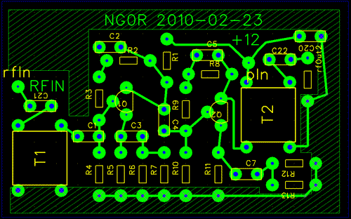
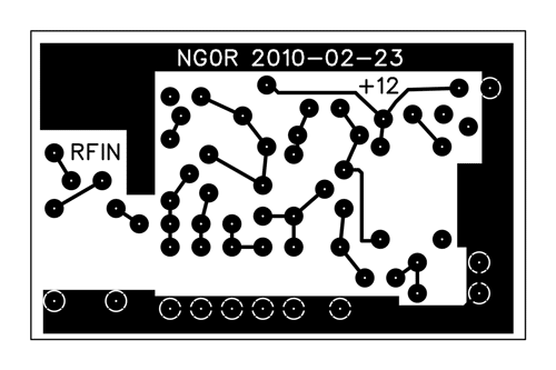
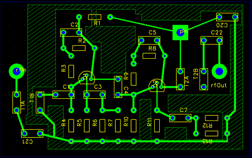
Tonight I converted the schematic to a layout for a printed circuit board.


I had several realizations tonight as I was laying this out.


  • I removed the parallel base resistors and replaced it with a single resistor.


    (I was battling a nightmare trying to route it on a single sided board when I realized
    that it was overkill and could be simplified. Wow... what a difference.)


  • I converted my 120 mil parts to 70 mil parts.

    (Now that my #67 drill bits have arrived I can work with much smaller pads even on
    home brew boards.)


  • The backplane of the board is now solid copper.

    (I have been wanting to test this and it was extremely simple.)


  • I figured out how to change the pilot hole size.

    (Used to center the drill bit)


  • I figured out how to change the size of the "copper-to-copper fill clearance"

    (15 mil looks pretty nice... I need to test it.)


  • I figured out how to change the "hole-edge to copper-fill clearance"

    (15 mil looks pretty nice... I need to test it.)


  • I can now route traces under/through other parts as needed as I start using smaller
    traces.


  • I expect this approach should etch much quicker as I am not removing nearly as much
    copper.


The new circuit board is remarkably simple compared to what I was playing with two
hours ago. Quite a few tweaks in my process as I spend some time bonding with FreePCB.


I think that this will probably one of three boards that I will try to etch on Saturday.


By:
Category:
Comments Off

Parallel Transistors - Night 2

I am not very happy with the way that this schematic looks.  I suppose that if I ponder it a while I can probably find a better way to visualize the circuit.


This is the same basic circuit as what I posted last night using the Java simulator.


Summary:


We have three small signal NPN transistors running in parallel. I think that you could
drop in a quite a few different parts with similar results. The bias on this is AC
on the base of the transistor. That means that it is only going to turn on for the
positive portion of the sign wave and when it cross zero and goes negative the transistor
is going to turn off. This should run in "class C" since there is no DC bias to the
base assuming that we are dealing with small signal parts.


This circuit is designed to be driven with about +10 to +20dBm with the parts as shown. 
I would expect that the input may need a transformer given that input is likely around
20 ohms depending on the size base resistors used. (Base resistor
/ 3 = Zin)
The output impedance of this is probably in the 200-300 ohm range
so T1 is used to match it to something in the 50 ohm range.


Running in "class C" the current to gain ratio is probably not too bad. Running in
"class A" this circuit would likely be extremely current hungry.


Plan:


I would like to try to make a board for this circuit and maybe a basic push-pull this
weekend


PS... Morning notes:


  • I updated the picture as I had an artifact in thee that I thought that I had moved...
    but I had grabbed the wrong image.


  • I added point of clarification in red
    (above)
    about the input impedance.


  • It was suggested that I could use three 150 resistors to get a Zin of approx 50 ohms.


  • When I did the software modeling (grain of salt) a 50-100 ohm base resistor looked
    slightly better over all in the circuit with about 10dBm of input drive.


  • During the software modeling (grain of salt again) a 100-200 ohm base resistor looked
    slightly better over all in the circuit with about 20dBm of input drive.


  • It will likely be either a transformer on a T50 size core or a base resistor of 50-200
    ohms either solution is cheap and easy depending on my mood and how it plays in the
    real world. (50-200 ohms will probably not play much differently. It is more likely
    going to be dependent on what parts I have on hand. I probably have 47, 51, and 100
    ohm parts in bulk but probably not many or any 150 ohm.)


By:
Category:
Comments Off

Parallel Transistors

I have seen several different pictures and schematics of some small signal transmitters that are using parallel NPNs to get 500-900mW of power. I keep running into these examples and they make me wonder.


I decided to try to put it into a simulator to see what it looks like.


Modeling:


This circuit is running in class C. The transistor base needs to be in 1.5-2 voltage
range which is between +10 to +15 dBm range with +20 dBm looking like the upper limit
as it starts getting current hungry in a hurry. I played with some different combinations
of resistors in the voltage divider and adding some DC bias to the base. The DC bias
could make it move into a different class beyond class C but the circuit got extremely
current hungry which makes sense. (Class C is fine for a CW rig with some good low
pass filtering.)


Plan:


I think that I will draw up this circuit in TinyCad and then move it into FreePCB
to eventually make printed circuit board. Once the board is etched and the parts are
stuffed I will measure and document it. I will then try to remodel this in software
(either in the Java based simulator or LTSpice) to see how the physical model and
software model compare.


Summary:


In the end this is a gimmick design using small signal parts like a PN2222 (2N2222A)
and/or a 2N3904 to push out some real power. It likely would be more productive and
stable to move this to a push-pull design and evaluate it based upon if it needs to
be in class AB or C depending it's intended use. The other option beyond a push-pull
design is to use a part that is somewhere between the "small signal" parts and the
"high power" parts as a driver or pre-driver, or even a "final" depending on the desired
power level.


With all of that being said... very high fun factor in the design and the software
modeling tonight.


73 de NG0R


By:
Category:
Comments Off

Dual Stage PN2222 Amp (Class A)

I have spent quite a bit of time this week exploring several different ideas:


  • Design a two stage amp (each stage with about 15db of gain)


  • Be stingy with the current budget


  • Convert the design into a home brew printed circuit board


  • Home brew the etchant


Here is the schematic that I put together. I moved one cap and replaced the 2N3094
NPNs with PN2222 (2N2222A) NPNs. I have a ton of PN2222 on hand so I would prefer
to use them up given how cheap they are.
I guessed that input was some where around
25 ohms and the output was about 150-250 ohms. The input and output tranformers are
wound to keep the overall circuit compatible with approx 50 ohms. (The circuit
is similar to the single stage circuit that I had been testing with.)


Here is the finished board. I etched the board Friday night after dinner and stuffed
the parts Sunday afternoon. The toriods are wound with left over CAT5 cable. The wire
is a nice size to work with on T50 cores.


Let's apply some power... nice... no smoke is released!


The graph below shows the that we are seeing almost 30dB of gain with drive levels
of -60dBm up to near -10dBm. The 2N3904 and PN2222 seem to lose gain near 0dBm of
drive input and this circuit follows that model. The current draw is about 58.8mA. 
This amp is running in Class A mode.


This circuit should be fine at any of the HF frequencies. I happen to be testing with
10.140MHz because I have a larger project that I am working on at that frequency.


  • The design is for wide band HF since there is no bandpass filter, lowpass filter,
    or tank circuit.


  • The PN2222 and 2N3904 are interchangeable in this design. I would suspect that there
    are quite a few other small signal NPN parts that you could drop in.


  • If you break this down and look at the first gain stage this design goes beyond a
    simple DC bias. C2 and R3 provide AC feedback in addition to the emitter with C3,
    R6, and R7.  Those two AC sections increase the gain and decrease the current
    consumed. Adding those components decreases the current consumption by about 20mA
    to get the same level of gain.


I have a oscillator and follower that is currently generating about -9dBm. Adding
this dual stage amp to the mentioned circuit would put this at approx +20dBm or 100mW
of RF. While that does not sound like huge power it is likely enough to feed a driver
or pre-driver stage for an amplifier.


Summary:


I meet all of the goals for this particular mini-project. I feel much more comfortable
putting together a design and making a home brew board that I am proud to show to
other people. A variation of this circuit will like make it into other projects in
the future.


73 de NG0R


By:
Category:
Comments Off

Someone else's QRSS MEPT STATION

Look at the PA circuit.


http://www.zianet.com/dhassall/QRSS.html


Kind of an interesting approach to a PA.


The image is lifted from the PDF. The PDF is
pretty hard to read.


At first glance I would have thought that it is current hungry. On closer inspection
it may not be running in class A. The base is running slightly above ground with no
DC. Depending on how much AC is on the base this looks like more of a B, AB, or C
design depending on the base voltage rise. The emitter is almost at ground with only
2.2 ohms of resistance.


It might be interesting to model this and then build as a simple circuit see the results.


By:
Category:
Comments Off

Mad Scientist Time - Making Printed Circuit Boards

Tonight was the highlight of the project.... mix some chemicals up and make the board!


Once again here is the schematic that I going to work with. (There is a minor change
or two on the board layout but it is pretty minor.) The schematic is laid out using
TinyCad. (Free/opensource software)


I found one or two minor issues with traces that I fixed after this image but this
is 99.5 what is on the board.

The board is laid out with FreePCB (Free/opensource).  From FreePCB I export
the CAM files into the Gerber format. I open the Gerber file with Viewmate from Pentalogix
(inexpensive program.) 


Tonight I took the project to the next level.


Steps:


  • I cut down a section of copper board & sanded the edges


  • I cleaned the board with a green cleaning pad and then rinsed it with acetone.


  • I printed out a template on the laser printer to register where the "print and peel"
    needed to be taped down to go thru the laser printer.


  • I printed a mirrored image on the print and peel (taped to a 8.5" x 11" sheet of paper.)


  • I attached  the small piece of "print & peel" paper to the copper board with
    masking tape.


  • I put the board & paper under my iron for about 60 seconds moving the iron around.


  • I ran the board & paper thru my GBC laminator twice.


  • I put the board & paper under my iron for about 60 seconds moving the iron around.


  • I ran the board & paper thru my GBC laminator twice.


  • I put the board & paper in a container filled with water for a couple of minutes.


  • I removed it from the water & then removed the tape and paper.


Next set of steps:


  • I touched up any holes or questionable spots with a Sharpie marker.


  • Put on the chemical gloves & safety glasses.


  • I then mixed up the chemicals in a Pyrex (glass) container. 1 part 3% Hydrogen Peroxide
    to 1 part Muriatic Acid.

    (The Muriatic acid is "hydrochloric acid" that can be purchased at a hardware store
    for $5 a gallon. It is used to clean pools, stone, car engines, etc. It is VERY strong
    so be careful.) Add the acid to the Hydrogen Peroxide to make sure that you don't
    have a run away exothermic reaction.


  • Drop the board in the Pyrex tray and agitate the tray every two minutes. (Warm chemicals
    will make the process go faster.)


  • My first board took about 12-15 minutes. I could probably cut it in 1/2 with the etchant
    at 100 degrees F.


  • Once the board is done rinse / soak the board in water while you clean up.


  • Pour the etchant into a plastic bottle (using a funnel) for reuse later for additional
    boards.


  • Rinse the Pyrex tray, funnel, bottles, gloves, etc under running water. Rinse out
    the sink REALLY well.


  • Remove the laser toner from the board with Acetone and a rag.


Ok I have to admit that initially I was going to only use the GBC laminator to heat
the board & paper. It did NOT get the board to the 300F/150C that is needed to
refuse the toner. It appears that this model only runs to 110C until it is hacked.
I am researching that piece but it appears that you replace a resistor in the thermistor
feedback circuit circuit. I am still looking for more detail as it would be nice to
loose the IRON set in this process.


I removed the toner from the laminator only test and reran the process with the steps
listed above.


Additional notes:


  • My first board has .020" traces with .120" pads. Since I am going to drill this with
    a small press I figured that I should make sure that I leave myself enough pad to
    work with. This board is only a single sided copper board.


  • I was worried that some of my traces would be undercut with the etchant. It was not
    an issue. I could easily have worked with .010" traces.


  • The process worked well enough that I could have used pin registration and two sheets
    of paper to make a double sided board.


  • I am now comfortable enough with TinyCad and FreePCB that I could crank out a schematic,
    board layout, and Gerber files for small/basic projects in an evening +/-.


73 de NG0R


By:
Category:
Comments Off

Laying out a PCB - Part 2

Here is the schematic from yesterday.


Here is an image of the updated single sided board layout.


  • I changed the resistors and capacitors with some self brewed parts in FreePCB. The
    new parts have 120 mil pads so that they can be drilled with a 1/16 drill. (I have
    smaller bits on order.)


  • I created a new NPN TO-92 part with the emitter, base, and collector layer the same
    as my PN2222 and 2N3904 layout. I created the parts with 120 mil pads.


  • I also created a part layout for some T50 toroids that will be used as the input and
    output transformers.


  • The area with the cross hatch is the copper ground on the empty space on the board.


The image below is what it will look like when I print on the "print and peel" transfer
paper. The only difference is that it will mirrored at the final printing. (The tool
that I am using to read the Gerber file has a mirror option in the printer settings.)


The image below shows what the silk screen would look like if I was going to send
it off to a commercial board shop. In my case I will just use it as a layout tool
when I plug in the parts.


I hope to etch the board on Saturday pending other family related duties & projects.


By:
Category:
Comments Off

Laying out a PCB

I want to test out a variation of a circuit to see how much gain it produces, how much current it consumes, how broadband that it is, and what drives levels work or don't work.


So tonight I laid out a schematic in TinyCad and had N0FP proof it for me via email/telephone.
(A second set of eyes is always helpful.)


I then imported the netlist into FreePCB. I decided to manually layout the parts and
route the connections since this is a single sided board. (You can use the autorouter
with boards that have two or more sides. But I am not ready to etch 2 side boards
yet.)  I took about an hour to route the board. That is not too bad for my first
serious attempt.


I did not get too radical routing ground and traces under other parts. This will be
the first board that I will be etching at my home so we need to start simple. The
hashed areas are additional ground plan that I added back to the board in the free
spaces.


I then exported the CAM files into Gerber and PNG formats.


How cool is that?    A better board would have a more complete ground
plan under the parts and/or use the second side as the ground plan to make it more
stable at RF frequencies. At HF this little 2 inch x 3 inch board should be just fine. (Yes,
I am aware that I will need to mirror the image before I transfer the toner to the
board.)


The real issue that I have is that I can't make the vias (holes) large enough for
me to comfortably drill them out with the tools that I have on hand. (It is likely
a software setting... I can change the trace width... just not the vias enough to
matter.) I do have some additional bits and a drill press type holder coming for my
dremel type tool. Hopefully the new bits will be small enough. (To cheat on this
board I might just open the image in GIMP and enlarge it a couple of percent so that
I can use the drill bits that I have on hand right now.... this is a prototype board
after all.)


A couple of lessons learned already:


  1. Consider making a two sided board. (Even if the second side is just a ground plane.)
    This will let you the auto router which will layout your parts and traces in a minute
    or two compared to 45-60 minutes manually. (You can always use the autorouter as a
    starting point and then manually convert it back to a single sided board.)


  2. Use the second side as a ground plane only. Drill thru to ground the parts where needed.


  3. Consider using surface mount parts where possible. It will conserve a lot of space
    and will reduce the amount of drilling that you may need to do. (I am not ready to
    move to SMT yet... but I can see where it might be nice in the future.)


This was an excellent experience tonight and I will do it again. I hope to try to
make the board sometime either this week or over the weekend.


73 de NG0R


PS.... I am looking at the layout and proofing it against the schematic. I just noticed
that the pin layout of Q1 & Q2 on board layout does not match the schematic. The
base and emitter are reversed on the board layout. Probably a variation in the T-92
part in the library. I can tweak that tomorrow in a couple of minutes so it is not
a big deal. :-) 


It might be a reason to try to run it through the autorouter to how that process
plays as a two sided board. (One side with parts and the other with a ground plane)


By:
Category:
Comments Off

Another quick 2N3904 test

I saw a schematic on the web that I wanted to validate....


The original article that I was reading suggested something like 15-17dB of gain.
I thought that was a little optimistic for a circuit with only DC bias. I expected
it to be current hungry and to be closer to 15dB of gain based upon some other tests
that I had run with similar components.


I did not go crazy with a wide range of test scenarios. The circuit is looking for
an input drive level of -10dBm to +10dBm. The circuit is pretty hungry at 57mA with
only 13.5 dBm of gain.


Some simple tweaks should be able to cut the current in half while pushing up the
gain some more while in class A operation.


Please see my notes at:

/Blog/PermaLink.aspx?guid=2de9126d-9ed0-4826-b14f-80f655ca5002


Oh yeah... I know that I need to come up with a bifilar transformer icon.  :-)


I had the parts on hand so it only took about 15 minutes to bread board it and
test it with the signal generator and power meter.