Laying out a PCB
I want to test out a variation of a circuit to see how much gain it produces, how much current it consumes, how broadband that it is, and what drives levels work or don't work.
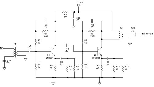
So tonight I laid out a schematic in TinyCad and had N0FP proof it for me via email/telephone.
(A second set of eyes is always helpful.)
I then imported the netlist into FreePCB. I decided to manually layout the parts and
route the connections since this is a single sided board. (You can use the autorouter
with boards that have two or more sides. But I am not ready to etch 2 side boards
yet.) I took about an hour to route the board. That is not too bad for my first
serious attempt.
I did not get too radical routing ground and traces under other parts. This will be
the first board that I will be etching at my home so we need to start simple. The
hashed areas are additional ground plan that I added back to the board in the free
spaces.
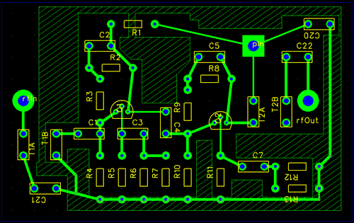
I then exported the CAM files into Gerber and PNG formats.

How cool is that? A better board would have a more complete ground
plan under the parts and/or use the second side as the ground plan to make it more
stable at RF frequencies. At HF this little 2 inch x 3 inch board should be just fine. (Yes,
I am aware that I will need to mirror the image before I transfer the toner to the
board.)
The real issue that I have is that I can't make the vias (holes) large enough for
me to comfortably drill them out with the tools that I have on hand. (It is likely
a software setting... I can change the trace width... just not the vias enough to
matter.) I do have some additional bits and a drill press type holder coming for my
dremel type tool. Hopefully the new bits will be small enough. (To cheat on this
board I might just open the image in GIMP and enlarge it a couple of percent so that
I can use the drill bits that I have on hand right now.... this is a prototype board
after all.)
A couple of lessons learned already:
This was an excellent experience tonight and I will do it again. I hope to try to
make the board sometime either this week or over the weekend.
73 de NG0R
PS.... I am looking at the layout and proofing it against the schematic. I just noticed
that the pin layout of Q1 & Q2 on board layout does not match the schematic. The
base and emitter are reversed on the board layout. Probably a variation in the T-92
part in the library. I can tweak that tomorrow in a couple of minutes so it is not
a big deal. :-)
It might be a reason to try to run it through the autorouter to how that process
plays as a two sided board. (One side with parts and the other with a ground plane)


So tonight I laid out a schematic in TinyCad and had N0FP proof it for me via email/telephone.
(A second set of eyes is always helpful.)
I then imported the netlist into FreePCB. I decided to manually layout the parts and
route the connections since this is a single sided board. (You can use the autorouter
with boards that have two or more sides. But I am not ready to etch 2 side boards
yet.) I took about an hour to route the board. That is not too bad for my first
serious attempt.
I did not get too radical routing ground and traces under other parts. This will be
the first board that I will be etching at my home so we need to start simple. The
hashed areas are additional ground plan that I added back to the board in the free
spaces.
I then exported the CAM files into Gerber and PNG formats.
How cool is that? A better board would have a more complete ground
plan under the parts and/or use the second side as the ground plan to make it more
stable at RF frequencies. At HF this little 2 inch x 3 inch board should be just fine. (Yes,
I am aware that I will need to mirror the image before I transfer the toner to the
board.)
The real issue that I have is that I can't make the vias (holes) large enough for
me to comfortably drill them out with the tools that I have on hand. (It is likely
a software setting... I can change the trace width... just not the vias enough to
matter.) I do have some additional bits and a drill press type holder coming for my
dremel type tool. Hopefully the new bits will be small enough. (To cheat on this
board I might just open the image in GIMP and enlarge it a couple of percent so that
I can use the drill bits that I have on hand right now.... this is a prototype board
after all.)
A couple of lessons learned already:
Consider making a two sided board. (Even if the second side is just a ground plane.)
This will let you the auto router which will layout your parts and traces in a minute
or two compared to 45-60 minutes manually. (You can always use the autorouter as a
starting point and then manually convert it back to a single sided board.)
Use the second side as a ground plane only. Drill thru to ground the parts where needed.
Consider using surface mount parts where possible. It will conserve a lot of space
and will reduce the amount of drilling that you may need to do. (I am not ready to
move to SMT yet... but I can see where it might be nice in the future.)
This was an excellent experience tonight and I will do it again. I hope to try to
make the board sometime either this week or over the weekend.
73 de NG0R
PS.... I am looking at the layout and proofing it against the schematic. I just noticed
that the pin layout of Q1 & Q2 on board layout does not match the schematic. The
base and emitter are reversed on the board layout. Probably a variation in the T-92
part in the library. I can tweak that tomorrow in a couple of minutes so it is not
a big deal. :-)
It might be a reason to try to run it through the autorouter to how that process
plays as a two sided board. (One side with parts and the other with a ground plane)