PCB Design
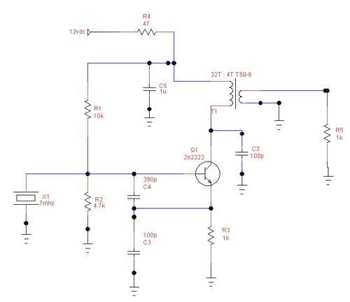
I spent some time
last night working on getting a schematic laid out in TinyCad.
I had a couple of issues that took me a little to resolve since it was my first time
laying something with it. Getting my ground to work as an actual ground and
then I had a couple of components where the wires would not properly connect even
though the junctions were good. I resolved all of the ground issues... and most
of the junction issues. I then exported it to a netlist and
partslist.
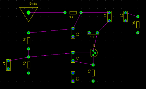
Next I moved on
to FreePCB. I was able to import
my netlist and
partslist right way. I then updated the package/footprint info and then started doing
the parts placement. The couple of places where I had junction issues came back as
an issue. I ended up just deleting the network for that connection and manually connected
the parts. Once a person figures that out it is a quick fix. I then decided that I
wanted a two sided board so that it would work with the autorouter software. I then
created a dsn file. (I used generic pads for the toroid based transformer.)
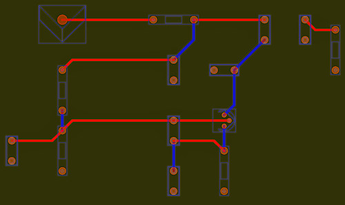
Next I opened the
dsn file with the Autorouter software. It laid out the connections in a couple
of seconds. The problem is that four of the traces were on the bottom of the board
which is an issue when I want to work on a one sided solder mask. I then exported
my updated dsn file and exported my spectra file.
dsn file with the Autorouter software. It laid out the connections in a couple
of seconds. The problem is that four of the traces were on the bottom of the board
which is an issue when I want to work on a one sided solder mask. I then exported
my updated dsn file and exported my spectra file.
Next I went back
to FreePCB and opened my updated
DSN and spectra files. I discovered that I can click on the traces and change them
back to top layer. That is a very cool hack to make my simple board a single sided
board again... traces on top... ground on the bottom. I then exported the CAM files
so that I would have some Gerber files to work with.
Next I opened up Viewmate and
opened up my Gerber
files. I was able to select my layer(s) and save them as BMPs or send them to
the laser printer or cutepdf. If I owned the app for the $49 I would have several other
options as well.

opened up my Gerber
files. I was able to select my layer(s) and save them as BMPs or send them to
the laser printer or cutepdf. If I owned the app for the $49 I would have several other
options as well.

I probably spent
4 hours end to end for my first time through the process. I could have easily made
a working "print & peel" or if I had a flatbed inkjet printed directly on a board.
Granted that my schematic was pretty simple but the process would have worked. I
did quick measurements and the capacitors that I ordered would have fit the pad
foot print on my board. The crystal pads should be adjusted to be a bit bigger
and the toroid pads probably should be spaced out a bit further as well.)
So overall I would
rate the experience as a B or B+ especially given that I am not an EE nor do
I have any experience with this kind of software or tools. (All of the software that I
used last night was open source or free.)
rate the experience as a B or B+ especially given that I am not an EE nor do
I have any experience with this kind of software or tools. (All of the software that I
used last night was open source or free.)

