By:
Category:
Comments Off

N2BEN + transverter + bench time


Ben (N2BEN... age 9) has been asking me for a few days if we could build a project
or kit again. (A sign that he either has "the knack" or cabin fever.) So tonight I
pushed my home brew projects a side pulled out my box of Elecraft
transverter kits
. I have a XV144 and XV432 that are awaiting some bench time to
get built. (I have a completed XV222 that I have been using for about 2 years.)


So tonight we started the XV144 kit. We sorted the components into project boxes for
temporary storage. We then assembled the front board. There are probably about 3 dozen
components. I read the directions and handed the parts to Ben and then he put the
parts onto the circuit board. We shared the soldering duties... he ran the iron and
I ran the solder.


We probably spend about 70 minutes tonight on the project.


It will be fun to plug these into the K2 once the project is done.


73 de NG0R


By:
Category:
Comments Off

Playing with PCBs and 2N7000 amps

I am planning on making some printed circuit boards this weekend. Since I need to get out the chemicals & related supplies I might as well make several boards.  So in addition to the board for the parallel NPN transistors I thought that I would make up some 2N7000 FET experiments as well.


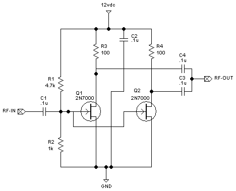
The circuit below is a dual FET design. The FETs are in parallel running in class
A. The Gate is biased for approximately 2 volts of DC drive with virtually no current
with assuming a bench power supply of 12-13.5 volts. (R3 and R4 are high values
for current limiting aka to avoid self destruction.)
The 2N7000 is rated for 200mA
of safe current. (200mA would suggest a drain resistor of approximately 68ohms.) I
don't really want to waste that much current but I want to see what this will draw.
I would prefer that it consume current less than my NPN experiments which is about
25mA per device with 15 to 17dB of gain per device. (I assume that I will be changing
the drain resistors once I know more about this FET.)


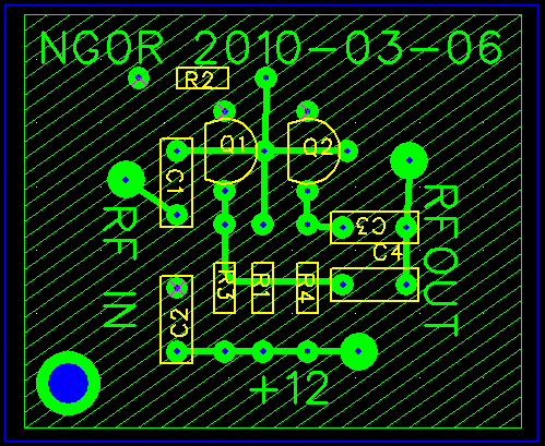
The image below shows what it looks like after spending a little bit of time bonding
with FreePCB.  (The blue circle in the bottom left is a small hole to hold/retrieve
the board in the etchant bath.)


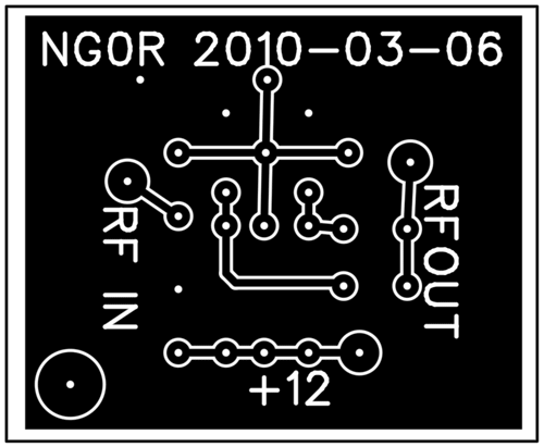
The image below shows what the copper will look like (in black.)   The white
areas will be removed by the etchant. The board looks big on the web but it is actually
only about 1.5 x 1.5 inches total. (If I removed the text and extra space it could
easily be condensed down to less than 1 x 1 inch.)


I don't know that I would would ever really use a design like this in the real world
but I want to get a feel for how it performs. I have NOT used FETs in any of my designs
or experiments yet so this is a good starting point.


Bipolar Junction Transistors are current devices. Field Effect Transistors are voltage
devices. It is interesting working with each of them as they have different design
considerations.


Some additional notes (before people start sending me emails):


  • The input impedance of this circuit is pretty high. It is not clear what high impedance
    is other than to say it could be way north of 1K. In this initial test I am not making
    any attempt to match the input. (That is why it is test.)


  • If I was going to try to match the input to something like my signal generator I would
    probably use a 1:4 or 1:5 turns ratio to take the 50 ohm source and transform it to
    between 800 and 1250 ohms.


  • The output of this should be approximately what the drain resistor value is. In this
    case it should see two 100 ohm resistors in parallel or 50 ohms. (I might be changing
    these resistors once I do some testing so it is a bit early to be too worried about
    matching the circuit. I would also need to now what the next circuit stage is that
    we need to integrate with.)
    It would be easy enough to wind a transformer on a
    T50-43 core to step-up/step-down as needed.


  • FETs are voltage sensitive.   Looking at the data sheet it appears that 60 volts
    is the max that the 2N7000 can handle. In a design for a "real" circuit it might be
    worth considering adding a zener diode to the drain to shunt off the excess voltage
    should it appear. (An example is running this circuit without having a load attached...
    it could spike the voltage on the drain to a fatal level. I have a limited number
    of 33 volt zeners on hand but that would potential for a design like this. For this
    test I am not going to worry about it. If I decide to use FETs in a "real" project
    I would probably include them.)


73 de NG0R


By:
Category:
Comments Off

USB-Powered Direct-Conversion Receiver

G1INF has an interesting example to demonstrate how simple a DC receiver can be.


http://g1inf.blogspot.com/2009/11/usb-powered-direct-conversion-receiver.html


I happen to have some SA602 on hand from a Mouser order that I placed last week. I
figured that it might be nice to have some on hand for some future projects. (I have
not worked on building any receivers yet as I am focused on simple oscillator driven
transmitters and how to build small signal gain stages at the moment.)


An interesting note in this blog post is that input impedance of the SA602 is 1500
ohms. I did not realize that but I have never really looked at the data sheet for
the SA602 in detail.


Here is a link to the datasheet:

http://www.nxp.com/documents/data_sheet/SA602A.pdf


Here are some of more interesting excerpts:


Good geeky stuff from the the blog world.


73 de NG0R


By:
Category:
Comments Off

Parallel Transistors - Night 3

Tonight I converted the schematic to a layout for a printed circuit board.


I had several realizations tonight as I was laying this out.


  • I removed the parallel base resistors and replaced it with a single resistor.


    (I was battling a nightmare trying to route it on a single sided board when I realized
    that it was overkill and could be simplified. Wow... what a difference.)


  • I converted my 120 mil parts to 70 mil parts.

    (Now that my #67 drill bits have arrived I can work with much smaller pads even on
    home brew boards.)


  • The backplane of the board is now solid copper.

    (I have been wanting to test this and it was extremely simple.)


  • I figured out how to change the pilot hole size.

    (Used to center the drill bit)


  • I figured out how to change the size of the "copper-to-copper fill clearance"

    (15 mil looks pretty nice... I need to test it.)


  • I figured out how to change the "hole-edge to copper-fill clearance"

    (15 mil looks pretty nice... I need to test it.)


  • I can now route traces under/through other parts as needed as I start using smaller
    traces.


  • I expect this approach should etch much quicker as I am not removing nearly as much
    copper.


The new circuit board is remarkably simple compared to what I was playing with two
hours ago. Quite a few tweaks in my process as I spend some time bonding with FreePCB.


I think that this will probably one of three boards that I will try to etch on Saturday.


By:
Category:
Comments Off

Parallel Transistors - Night 2

I am not very happy with the way that this schematic looks.  I suppose that if I ponder it a while I can probably find a better way to visualize the circuit.


This is the same basic circuit as what I posted last night using the Java simulator.


Summary:


We have three small signal NPN transistors running in parallel. I think that you could
drop in a quite a few different parts with similar results. The bias on this is AC
on the base of the transistor. That means that it is only going to turn on for the
positive portion of the sign wave and when it cross zero and goes negative the transistor
is going to turn off. This should run in "class C" since there is no DC bias to the
base assuming that we are dealing with small signal parts.


This circuit is designed to be driven with about +10 to +20dBm with the parts as shown. 
I would expect that the input may need a transformer given that input is likely around
20 ohms depending on the size base resistors used. (Base resistor
/ 3 = Zin)
The output impedance of this is probably in the 200-300 ohm range
so T1 is used to match it to something in the 50 ohm range.


Running in "class C" the current to gain ratio is probably not too bad. Running in
"class A" this circuit would likely be extremely current hungry.


Plan:


I would like to try to make a board for this circuit and maybe a basic push-pull this
weekend


PS... Morning notes:


  • I updated the picture as I had an artifact in thee that I thought that I had moved...
    but I had grabbed the wrong image.


  • I added point of clarification in red
    (above)
    about the input impedance.


  • It was suggested that I could use three 150 resistors to get a Zin of approx 50 ohms.


  • When I did the software modeling (grain of salt) a 50-100 ohm base resistor looked
    slightly better over all in the circuit with about 10dBm of input drive.


  • During the software modeling (grain of salt again) a 100-200 ohm base resistor looked
    slightly better over all in the circuit with about 20dBm of input drive.


  • It will likely be either a transformer on a T50 size core or a base resistor of 50-200
    ohms either solution is cheap and easy depending on my mood and how it plays in the
    real world. (50-200 ohms will probably not play much differently. It is more likely
    going to be dependent on what parts I have on hand. I probably have 47, 51, and 100
    ohm parts in bulk but probably not many or any 150 ohm.)


By:
Category:
Comments Off

Parallel Transistors

I have seen several different pictures and schematics of some small signal transmitters that are using parallel NPNs to get 500-900mW of power. I keep running into these examples and they make me wonder.


I decided to try to put it into a simulator to see what it looks like.


Modeling:


This circuit is running in class C. The transistor base needs to be in 1.5-2 voltage
range which is between +10 to +15 dBm range with +20 dBm looking like the upper limit
as it starts getting current hungry in a hurry. I played with some different combinations
of resistors in the voltage divider and adding some DC bias to the base. The DC bias
could make it move into a different class beyond class C but the circuit got extremely
current hungry which makes sense. (Class C is fine for a CW rig with some good low
pass filtering.)


Plan:


I think that I will draw up this circuit in TinyCad and then move it into FreePCB
to eventually make printed circuit board. Once the board is etched and the parts are
stuffed I will measure and document it. I will then try to remodel this in software
(either in the Java based simulator or LTSpice) to see how the physical model and
software model compare.


Summary:


In the end this is a gimmick design using small signal parts like a PN2222 (2N2222A)
and/or a 2N3904 to push out some real power. It likely would be more productive and
stable to move this to a push-pull design and evaluate it based upon if it needs to
be in class AB or C depending it's intended use. The other option beyond a push-pull
design is to use a part that is somewhere between the "small signal" parts and the
"high power" parts as a driver or pre-driver, or even a "final" depending on the desired
power level.


With all of that being said... very high fun factor in the design and the software
modeling tonight.


73 de NG0R


By:
Category:
Comments Off

Dual Stage PN2222 Amp (Class A)

I have spent quite a bit of time this week exploring several different ideas:


  • Design a two stage amp (each stage with about 15db of gain)


  • Be stingy with the current budget


  • Convert the design into a home brew printed circuit board


  • Home brew the etchant


Here is the schematic that I put together. I moved one cap and replaced the 2N3094
NPNs with PN2222 (2N2222A) NPNs. I have a ton of PN2222 on hand so I would prefer
to use them up given how cheap they are.
I guessed that input was some where around
25 ohms and the output was about 150-250 ohms. The input and output tranformers are
wound to keep the overall circuit compatible with approx 50 ohms. (The circuit
is similar to the single stage circuit that I had been testing with.)


Here is the finished board. I etched the board Friday night after dinner and stuffed
the parts Sunday afternoon. The toriods are wound with left over CAT5 cable. The wire
is a nice size to work with on T50 cores.


Let's apply some power... nice... no smoke is released!


The graph below shows the that we are seeing almost 30dB of gain with drive levels
of -60dBm up to near -10dBm. The 2N3904 and PN2222 seem to lose gain near 0dBm of
drive input and this circuit follows that model. The current draw is about 58.8mA. 
This amp is running in Class A mode.


This circuit should be fine at any of the HF frequencies. I happen to be testing with
10.140MHz because I have a larger project that I am working on at that frequency.


  • The design is for wide band HF since there is no bandpass filter, lowpass filter,
    or tank circuit.


  • The PN2222 and 2N3904 are interchangeable in this design. I would suspect that there
    are quite a few other small signal NPN parts that you could drop in.


  • If you break this down and look at the first gain stage this design goes beyond a
    simple DC bias. C2 and R3 provide AC feedback in addition to the emitter with C3,
    R6, and R7.  Those two AC sections increase the gain and decrease the current
    consumed. Adding those components decreases the current consumption by about 20mA
    to get the same level of gain.


I have a oscillator and follower that is currently generating about -9dBm. Adding
this dual stage amp to the mentioned circuit would put this at approx +20dBm or 100mW
of RF. While that does not sound like huge power it is likely enough to feed a driver
or pre-driver stage for an amplifier.


Summary:


I meet all of the goals for this particular mini-project. I feel much more comfortable
putting together a design and making a home brew board that I am proud to show to
other people. A variation of this circuit will like make it into other projects in
the future.


73 de NG0R


By:
Category:
Comments Off

Someone else's QRSS MEPT STATION

Look at the PA circuit.


http://www.zianet.com/dhassall/QRSS.html


Kind of an interesting approach to a PA.


The image is lifted from the PDF. The PDF is
pretty hard to read.


At first glance I would have thought that it is current hungry. On closer inspection
it may not be running in class A. The base is running slightly above ground with no
DC. Depending on how much AC is on the base this looks like more of a B, AB, or C
design depending on the base voltage rise. The emitter is almost at ground with only
2.2 ohms of resistance.


It might be interesting to model this and then build as a simple circuit see the results.


By:
Category:
Comments Off

Mad Scientist Time - Making Printed Circuit Boards

Tonight was the highlight of the project.... mix some chemicals up and make the board!


Once again here is the schematic that I going to work with. (There is a minor change
or two on the board layout but it is pretty minor.) The schematic is laid out using
TinyCad. (Free/opensource software)


I found one or two minor issues with traces that I fixed after this image but this
is 99.5 what is on the board.

The board is laid out with FreePCB (Free/opensource).  From FreePCB I export
the CAM files into the Gerber format. I open the Gerber file with Viewmate from Pentalogix
(inexpensive program.) 


Tonight I took the project to the next level.


Steps:


  • I cut down a section of copper board & sanded the edges


  • I cleaned the board with a green cleaning pad and then rinsed it with acetone.


  • I printed out a template on the laser printer to register where the "print and peel"
    needed to be taped down to go thru the laser printer.


  • I printed a mirrored image on the print and peel (taped to a 8.5" x 11" sheet of paper.)


  • I attached  the small piece of "print & peel" paper to the copper board with
    masking tape.


  • I put the board & paper under my iron for about 60 seconds moving the iron around.


  • I ran the board & paper thru my GBC laminator twice.


  • I put the board & paper under my iron for about 60 seconds moving the iron around.


  • I ran the board & paper thru my GBC laminator twice.


  • I put the board & paper in a container filled with water for a couple of minutes.


  • I removed it from the water & then removed the tape and paper.


Next set of steps:


  • I touched up any holes or questionable spots with a Sharpie marker.


  • Put on the chemical gloves & safety glasses.


  • I then mixed up the chemicals in a Pyrex (glass) container. 1 part 3% Hydrogen Peroxide
    to 1 part Muriatic Acid.

    (The Muriatic acid is "hydrochloric acid" that can be purchased at a hardware store
    for $5 a gallon. It is used to clean pools, stone, car engines, etc. It is VERY strong
    so be careful.) Add the acid to the Hydrogen Peroxide to make sure that you don't
    have a run away exothermic reaction.


  • Drop the board in the Pyrex tray and agitate the tray every two minutes. (Warm chemicals
    will make the process go faster.)


  • My first board took about 12-15 minutes. I could probably cut it in 1/2 with the etchant
    at 100 degrees F.


  • Once the board is done rinse / soak the board in water while you clean up.


  • Pour the etchant into a plastic bottle (using a funnel) for reuse later for additional
    boards.


  • Rinse the Pyrex tray, funnel, bottles, gloves, etc under running water. Rinse out
    the sink REALLY well.


  • Remove the laser toner from the board with Acetone and a rag.


Ok I have to admit that initially I was going to only use the GBC laminator to heat
the board & paper. It did NOT get the board to the 300F/150C that is needed to
refuse the toner. It appears that this model only runs to 110C until it is hacked.
I am researching that piece but it appears that you replace a resistor in the thermistor
feedback circuit circuit. I am still looking for more detail as it would be nice to
loose the IRON set in this process.


I removed the toner from the laminator only test and reran the process with the steps
listed above.


Additional notes:


  • My first board has .020" traces with .120" pads. Since I am going to drill this with
    a small press I figured that I should make sure that I leave myself enough pad to
    work with. This board is only a single sided copper board.


  • I was worried that some of my traces would be undercut with the etchant. It was not
    an issue. I could easily have worked with .010" traces.


  • The process worked well enough that I could have used pin registration and two sheets
    of paper to make a double sided board.


  • I am now comfortable enough with TinyCad and FreePCB that I could crank out a schematic,
    board layout, and Gerber files for small/basic projects in an evening +/-.


73 de NG0R