By:
Category:
Comments Off

Laying out a PCB - Part 2

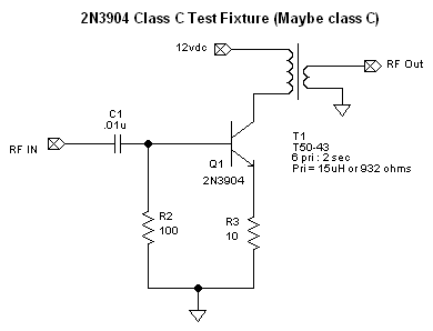
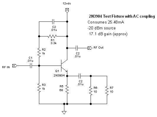
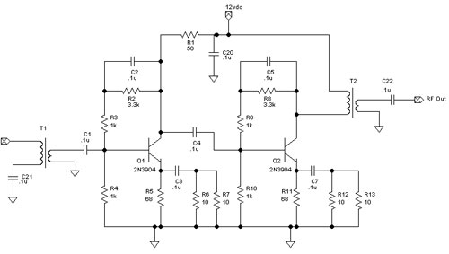
Here is the schematic from yesterday.


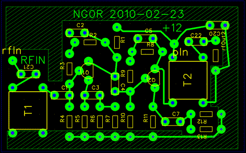
Here is an image of the updated single sided board layout.


  • I changed the resistors and capacitors with some self brewed parts in FreePCB. The
    new parts have 120 mil pads so that they can be drilled with a 1/16 drill. (I have
    smaller bits on order.)


  • I created a new NPN TO-92 part with the emitter, base, and collector layer the same
    as my PN2222 and 2N3904 layout. I created the parts with 120 mil pads.


  • I also created a part layout for some T50 toroids that will be used as the input and
    output transformers.


  • The area with the cross hatch is the copper ground on the empty space on the board.


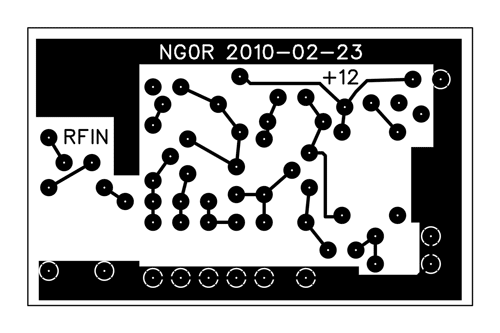
The image below is what it will look like when I print on the "print and peel" transfer
paper. The only difference is that it will mirrored at the final printing. (The tool
that I am using to read the Gerber file has a mirror option in the printer settings.)


The image below shows what the silk screen would look like if I was going to send
it off to a commercial board shop. In my case I will just use it as a layout tool
when I plug in the parts.


I hope to etch the board on Saturday pending other family related duties & projects.
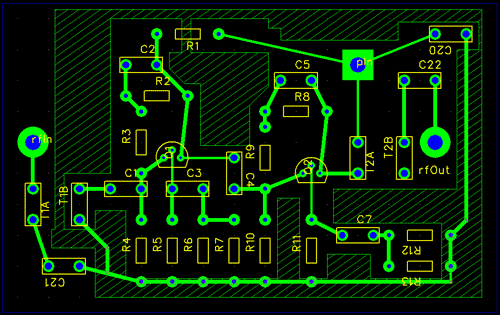


By:
Category:
Comments Off

Laying out a PCB

I want to test out a variation of a circuit to see how much gain it produces, how much current it consumes, how broadband that it is, and what drives levels work or don't work.


So tonight I laid out a schematic in TinyCad and had N0FP proof it for me via email/telephone.
(A second set of eyes is always helpful.)


I then imported the netlist into FreePCB. I decided to manually layout the parts and
route the connections since this is a single sided board. (You can use the autorouter
with boards that have two or more sides. But I am not ready to etch 2 side boards
yet.)  I took about an hour to route the board. That is not too bad for my first
serious attempt.


I did not get too radical routing ground and traces under other parts. This will be
the first board that I will be etching at my home so we need to start simple. The
hashed areas are additional ground plan that I added back to the board in the free
spaces.


I then exported the CAM files into Gerber and PNG formats.


How cool is that?    A better board would have a more complete ground
plan under the parts and/or use the second side as the ground plan to make it more
stable at RF frequencies. At HF this little 2 inch x 3 inch board should be just fine. (Yes,
I am aware that I will need to mirror the image before I transfer the toner to the
board.)


The real issue that I have is that I can't make the vias (holes) large enough for
me to comfortably drill them out with the tools that I have on hand. (It is likely
a software setting... I can change the trace width... just not the vias enough to
matter.) I do have some additional bits and a drill press type holder coming for my
dremel type tool. Hopefully the new bits will be small enough. (To cheat on this
board I might just open the image in GIMP and enlarge it a couple of percent so that
I can use the drill bits that I have on hand right now.... this is a prototype board
after all.)


A couple of lessons learned already:


  1. Consider making a two sided board. (Even if the second side is just a ground plane.)
    This will let you the auto router which will layout your parts and traces in a minute
    or two compared to 45-60 minutes manually. (You can always use the autorouter as a
    starting point and then manually convert it back to a single sided board.)


  2. Use the second side as a ground plane only. Drill thru to ground the parts where needed.


  3. Consider using surface mount parts where possible. It will conserve a lot of space
    and will reduce the amount of drilling that you may need to do. (I am not ready to
    move to SMT yet... but I can see where it might be nice in the future.)


This was an excellent experience tonight and I will do it again. I hope to try to
make the board sometime either this week or over the weekend.


73 de NG0R


PS.... I am looking at the layout and proofing it against the schematic. I just noticed
that the pin layout of Q1 & Q2 on board layout does not match the schematic. The
base and emitter are reversed on the board layout. Probably a variation in the T-92
part in the library. I can tweak that tomorrow in a couple of minutes so it is not
a big deal. :-) 


It might be a reason to try to run it through the autorouter to how that process
plays as a two sided board. (One side with parts and the other with a ground plane)


By:
Category:
Comments Off

Another quick 2N3904 test

I saw a schematic on the web that I wanted to validate....


The original article that I was reading suggested something like 15-17dB of gain.
I thought that was a little optimistic for a circuit with only DC bias. I expected
it to be current hungry and to be closer to 15dB of gain based upon some other tests
that I had run with similar components.


I did not go crazy with a wide range of test scenarios. The circuit is looking for
an input drive level of -10dBm to +10dBm. The circuit is pretty hungry at 57mA with
only 13.5 dBm of gain.


Some simple tweaks should be able to cut the current in half while pushing up the
gain some more while in class A operation.


Please see my notes at:

/Blog/PermaLink.aspx?guid=2de9126d-9ed0-4826-b14f-80f655ca5002


Oh yeah... I know that I need to come up with a bifilar transformer icon.  :-)


I had the parts on hand so it only took about 15 minutes to bread board it and
test it with the signal generator and power meter.


By:
Category:
Comments Off

Transistors: Classes A, AB, B, and C

I am still reading and trying to figure out the differences in how each class is biased.


Class A is the most common example and pretty well documented:


  • R3 is controlling the majority of the current for the device


  • R1 & R2 are a DC voltage divider probably about ~1/2 the Voltage at the collector


  • T1 (which could also be a resistor) at the Q1 collector is ~ 1/2 Vcc


  • Tweak the R3 / T1 (or the resistor substitute or T1) ratio drive your power output.


  • Current hungry circuit.


  • Can easily get 10, 15, and approaching 20dB of gain


  • I am seeing 17dB of gain with 25mA with some additional AC feedback at the emitter,
    and between the collector and base.


  • The amp is running 100% duty cycle.


------------------------


Class AB or B is discussed in detail but very few math examples:


  • Configure R1 & R2 for about 0.7v. This will largely determine what class you are
    in. The higher the voltage the more likely you are to be in class AB or A. The lower
    the voltage the closer to B or even C.


  • R3 is largely controlling the device current


  • T1 (which could also become a resistor) is being used to transform the output to match
    the next stage. 


  • The amp is running between around 50% duty cycle.


  • Normally this is used in a push-pull pair.


  • AB in a push-pull pair can have some cross-over distortion because there is a period
    of time in the sine wave where there is no signal when both transistors are in the
    off state.


  • Can be used for audio or SSB circuits as there is little distortion especially in
    class B.


------------------------


Class C is discussed in detail but very few math examples:


  • Set R3 for current level of the device


  • R2 serves as a wideband load for the input driver. Decreasing
    this resistance can improve stability at the price of gain.


  • The base only turns on when there is enough positive drive.


  • The duty cycle is less than 50%


  • Should only be used for CW or FM given the distortion in the sine wave.


  • Could be harmonic rich so output filter needs to be investigated.


  • T1 (which could also become a resistor) is being used to transform the output to match
    the next stage.


  • I will design T1 for a 200 ohm to 50 ohm match. This is just
    a shot in the dark initially but I need a starting point to test with. A T50-61 toroid
    with 7 turns on the primary and 3 turns on the secondary will provide a transformation
    of 220 ohms to 40 ohms.  At 10MHz a T50-61 toriod with 7 turns is z=220, L=3.5uH,
    C=72pF.


  • The input of this circuit is probably low impedance. For
    my initial testing I will probably build a 50 ohm to 12 ohm transformer and see if
    that helps. (I am using my signal generator for my initial testing which is 50 ohms.
    I will probably use 8 turns to 4 turns on a T50-43 or T50-61 core.)


  • EMRFD suggests using a Zener diode at the collector that
    is 3x the Vcc value but less than the transistor break down. The idea is to prevent
    the transistor from self destructing at extreme voltage peaks while otherwise being
    largely invisible to the circuit.


------------------------


Open Questions:


  • In class AB, B, and C how should we be be calculating the amount of current that we
    designing for?


  • How should we be sizing T1?


    T1 shown in the examples above is functioning as an RF choke, collector resistor,
    and output transformer. (Lots of value from that one part.)   The examples
    that I have seen don't include much math or reasoning. It would seem like there is
    some current limiting happening in T1 acting as a resistor that should be factored
    in.


  • How does the R2 (base current) and T1 (collector current) ratio interact?


  • How do we model/suggest/approximate the power gain in these designs?


I will try to come back and update this post with additional notes & corrections
as I learn more.


By:
Category:
Comments Off

Trying to figure out class C for a 2N3904

I am a bit confused.....  I am trying to test something that I saw in a book.

(That is generally how trouble begins)


I am trying to test getting a 2N3904 into class c operation. The challenge is that
I can't find an example of the math to calculate how to get to class C. (Most examples
are focused on class A operation.)  So I built the circuit on a bread board and
applied power and then some RF from my signal generator.


The image from the oscope shows the collector in the upper waveform and the base on
the lower wave form. The divisions are .5v and the probes are set to 10x.


Vcc is 12.5v

Base is about 10v

Collector is about 43v

This is with +20dBm source drive connected to the base.


That is funny... I am banging on that transistor pretty hard. I should look up
the max power for the part. I am probably approaching the fatal value.  
--The visual was good for the photo to show the class C waveform..   :-)


My results were.... ummm... poor!   It makes a really nice attenuator.


It appears that the transistor is NOT turning on until it gets +10dBm of drive. When
it does turn on it is not very efficient at +2dB of gain.  (I was getting 17dB
of gain with 25mA of current in class A a couple of nights ago.)


Positive:


When I added the transformer I did reduce the amount of loading on transistor. It
was nice to be able to see the before and after effects of that on the oscope.


Negative:


It is clear that I need to read some more on this topic as it did not play out the
way that the initial reading might suggest.


Frustration:


I am having a hard time find an example of math model that gives some feel for how
to bias into the various classes beyond class A. (Almost all of the examples are class
A.) When you start moving beyond it into AB & C they start to drop off the math
details and direct you into the push-pull model. (I will eventually get to push-pull..
but I want to understand how it works with one transistor before I try to match up
two of them.)


Next steps:


Try to dig deeper into the bias issue. (It is probably very simple once I understand
this in more detail.)


PS... I updated the post to include an oscope picture of the waveforms.


By:
Category:
Comments Off

Alan Yates - 30m QRSS beacon

Alan has a neat site with lots of details on how he built his 30m QRSS beacon.  http://www.vk2zay.net/article/181


I like Alan's thinking. You spend a lot of noodling thru math & variables as you
work thru these circuit designs. Alan has put many of his calculators online.  http://www.vk2zay.net/calculators/


So far I have been putting my calculators into a spreadsheet. It is easy and to be
real honest I don't always trust the calculators so I am little reluctant to publish
them until I have done some testing and have some faith in model. Granted they are
just a tool to point you in the general direction as the results in the real world
might vary a bit.


Back to the QRSS project for a minute. It is interesting looking at Alan's site. I
am also playing with 2N3904 and 2N7000 parts and pondering the use of varactor diodes
to swing the tuning. I planning to use a PIC for the keying but the the Atmel family
is another popular solution.


Fun reading.


73 de NG0R


By:
Category:
Comments Off

30m Oscillator (Night 9)

I am trying to squeeze in a few minutes of knack time after work and before dinner.


I started putting some of the components of my project into LTSpice.  Right now
I just have the oscillator, follower, and the lowpass filter in the circuit. I am
see unity gain at the moment but that is expected since there is no gain stage in
the circuit yet. I plan to extend the model a bit a see what it might look like with
some gain.


It will be interesting to see how this plays. I should model this out and then build
a new board and compare the results. (Maybe... depends on how the weekend plays out.)


I have some supplies on order so that I can start making printed circuit boards in
addition to Manhattan Pad construction and Island construction. The island construction
method is pretty quick but it is hard to drive much density compared to a pcb laid
out on the computer and run thru the laser printer & toner transfer process.


73 de NG0R


By:
Category:
Comments Off

30m Oscillator (Night 8)

For tonight the theme was trying to get more gain with less current. (This is a theme over the past several nights.)


So I started poking around in Experimental Methods in RF Design... it is pleasure
reading for knack victims. As I started browsing through Chapter 2 intending to read
up on push-pull amps I stumbled across some interesting notes. It was almost a eureka
moment except that I don't understand exactly how to calculate the target RF power
levels yet.


So far I have been largely focused on creating power based upon the DC biased values.
That is important but it does not maximize RF gain and is not as efficient as I might
like it to be. I was getting ~14.6 dBm of gain at a cost of 35mA which is not brilliant.
In the book I noticed a design almost the same as I what I have been working with
but getting almost 20dBm of gain at 20mA.


The difference in the two designs was simple:


1. Don't drive the DC design nearly as hard... I was throwing current at the problem
in brute force fashion.

2. Think about RF.... use some AC coupled feedback to create the gain.


The schematic above is my first attempt to bread board out the idea in the book against
my world and collection of available parts. It looks a LOT like the previous designs
except it is a lower current design with AC coupling between the collector/base and
at the emitter.


Now that I own a nice power meter I ran some tests and captured data.


I measured my signal generator with my power meter, then took down some base values,
and then reran the same test with the 2N3904 amp circuit. I did a little spreadsheet
magic to calculate the gain and then built a graph with the results.


Highlights:


  • I can generate about 16-17dBm of gain with about 25mA of power. (That is +3dBm and
    -10mA from the previous tests with no AC feedback and strictly DC bias.)


  • The gain is pretty consistent with -50 to -10dBm of drive source.


  • The gain falls off very quickly at 0dBm of drive.


  • As the gain falls off the amp begins to consume a lot of current to produce a small
    amount of gain.


  • The 2N2222 and 2N3904 appear to be good up to about 0dBm of input signal and then
    loose their effectiveness. They willl be driving up the harmonic content instead of
    the fundamental signal. (I visually saw & measured this on my spectrum analyzer
    over the past several nights of testing.)


In theory I could probably tweak the resistor values to drive another 2-3dBm of gain
& use a transformer at the RF output to reduce the loading and create a better
match.


In reality I have a good predriver circuit and need to look at some other options
for the next gain stage. (Things like class AB or class C, push-pull amps, or simply
some different parts as I start to transition out of small signal components and into
power.)


Tons of learning tonight. I feel pretty positive about the results. I need to dig
in and better understand the concept of feedback in an amplifier. (35 minutes at the
work bench.  2 hours at the PC working the data and documenting the results.)


73 de NG0R


PS... a quick follow up note after the initial post


I think that the output impedance of this is ~156 ohms.

Ie = Ve / Re  or .053 = 3.66/68  (ohms law)

Zout = (Vcc-Vb) / Ie


155.6 = (12.61-4.36)/.053    


156 ohms would make sense... you see a lot of these circuits using a 4:1 transformer.
That will transform 200 ohms to 50 ohms which is in the ball park.


PPS... another thought from yesterday's reading & bench time


Rf * Re = Rs * Rl  or  Rf * Re = Zin & Zout


Rf & Re are the AC coupled components.
(updated below... Re is the total of Re + RE)


In my schematic above I probably should switch the 1K and 3.3K resistors between the
collector and base. That would set  Zin to 50 and Zout of 200 approximately. 
Something to test. (This is designed for 200 ohms at the moment.)


PPPS.... more math


Rf is the parallel feedback resistor (the AC path)


Re
is the net of Re + RE  (Re is the DC bias + RE is the AC
degeneration)

Zin & Zout (Input and output impedance.)