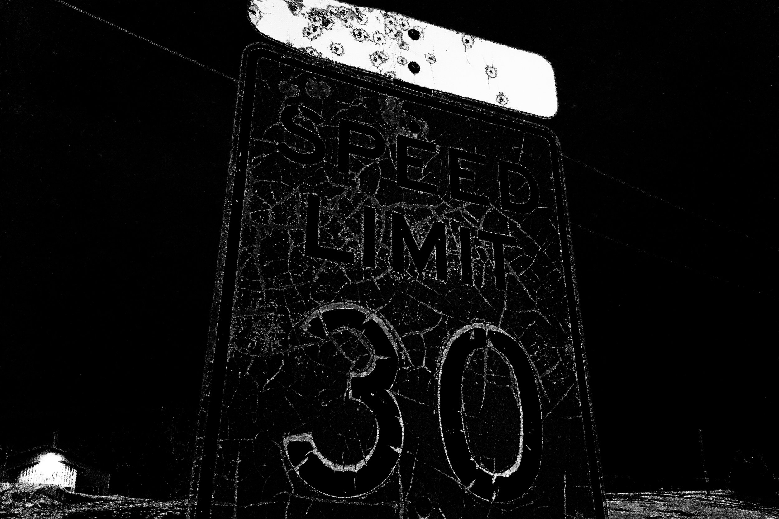
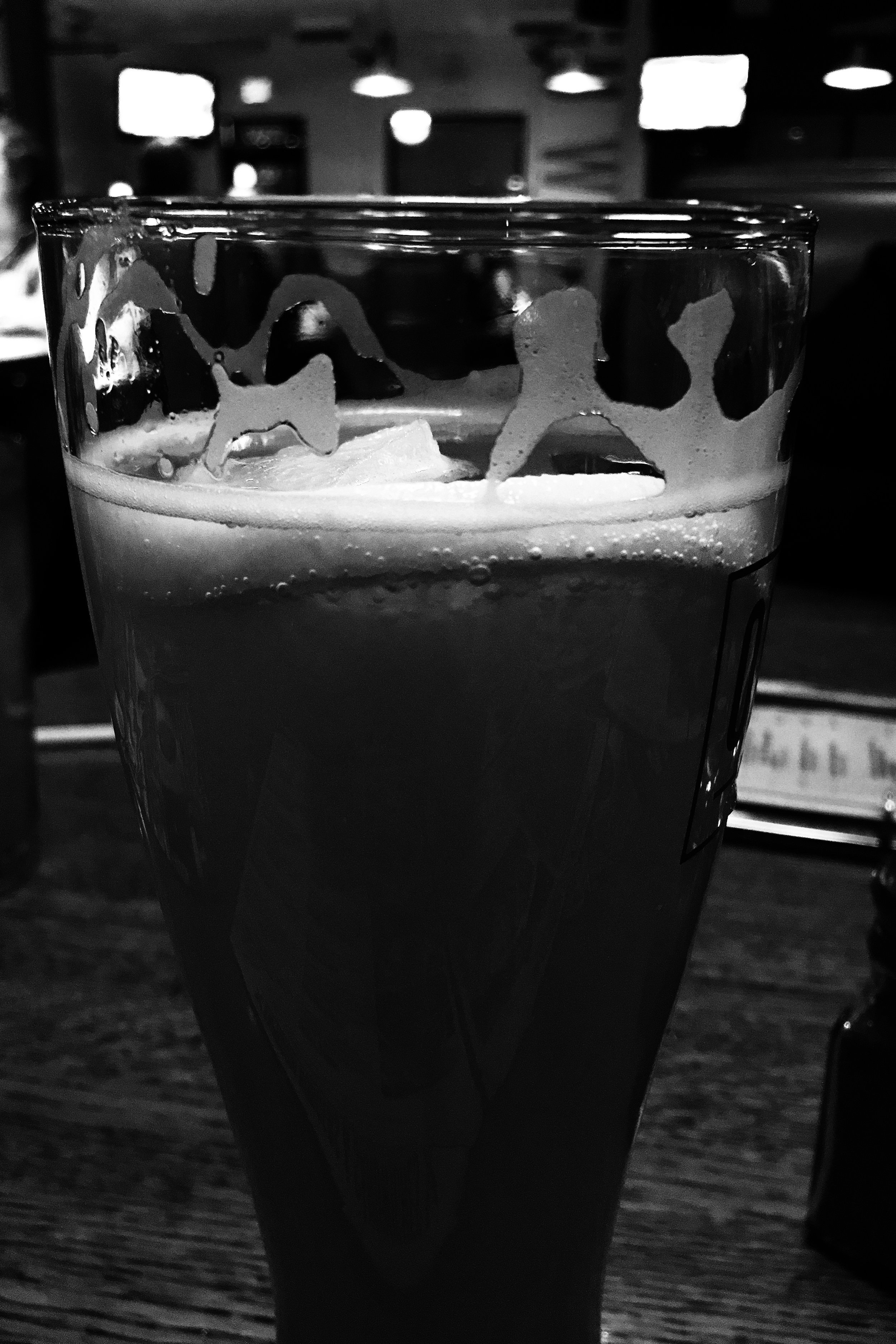
Random sighting
A quick trip to town
A quick trip to town
A quick walk with Max the Wonder Dog
Wednesday after work

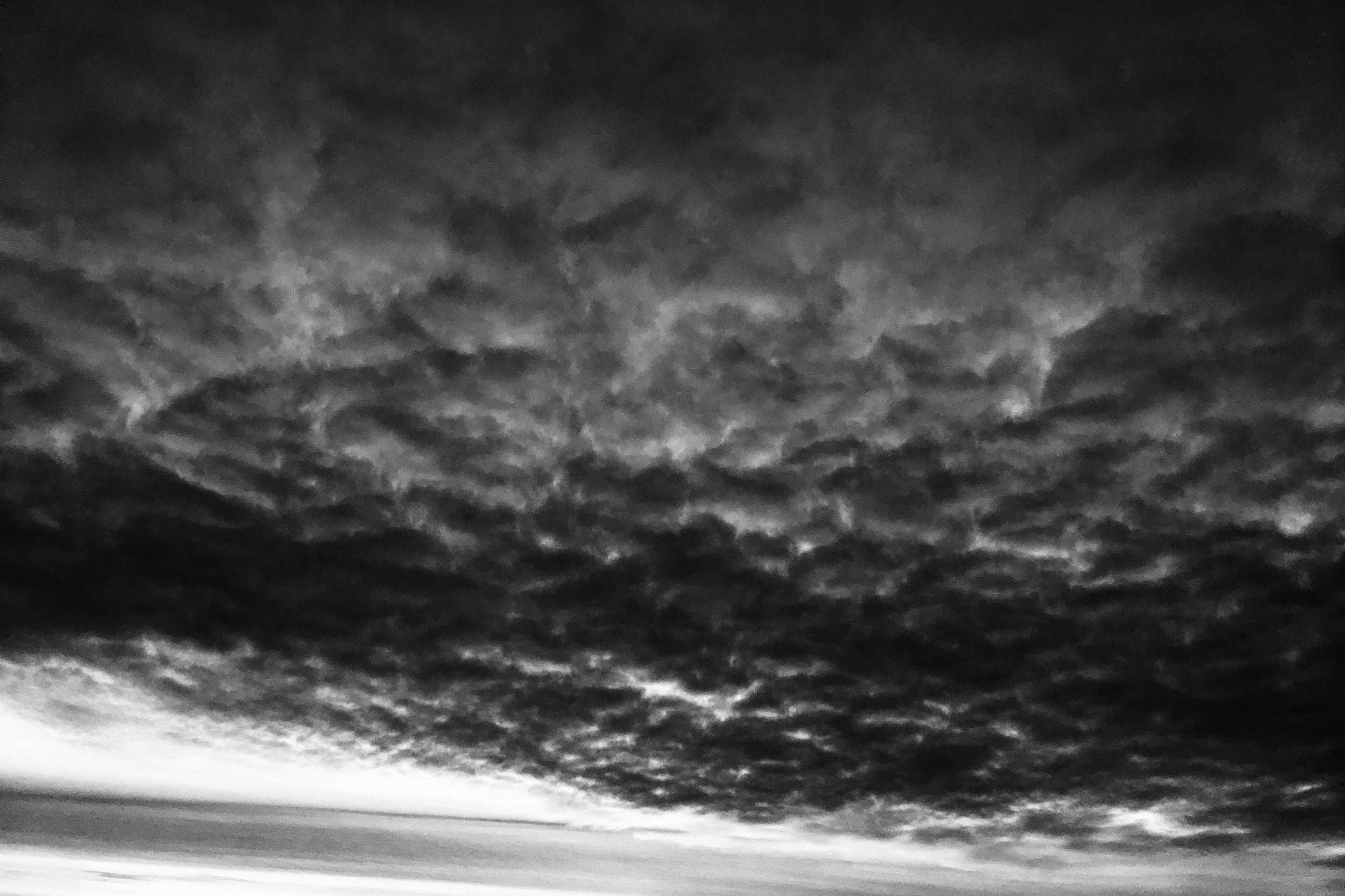
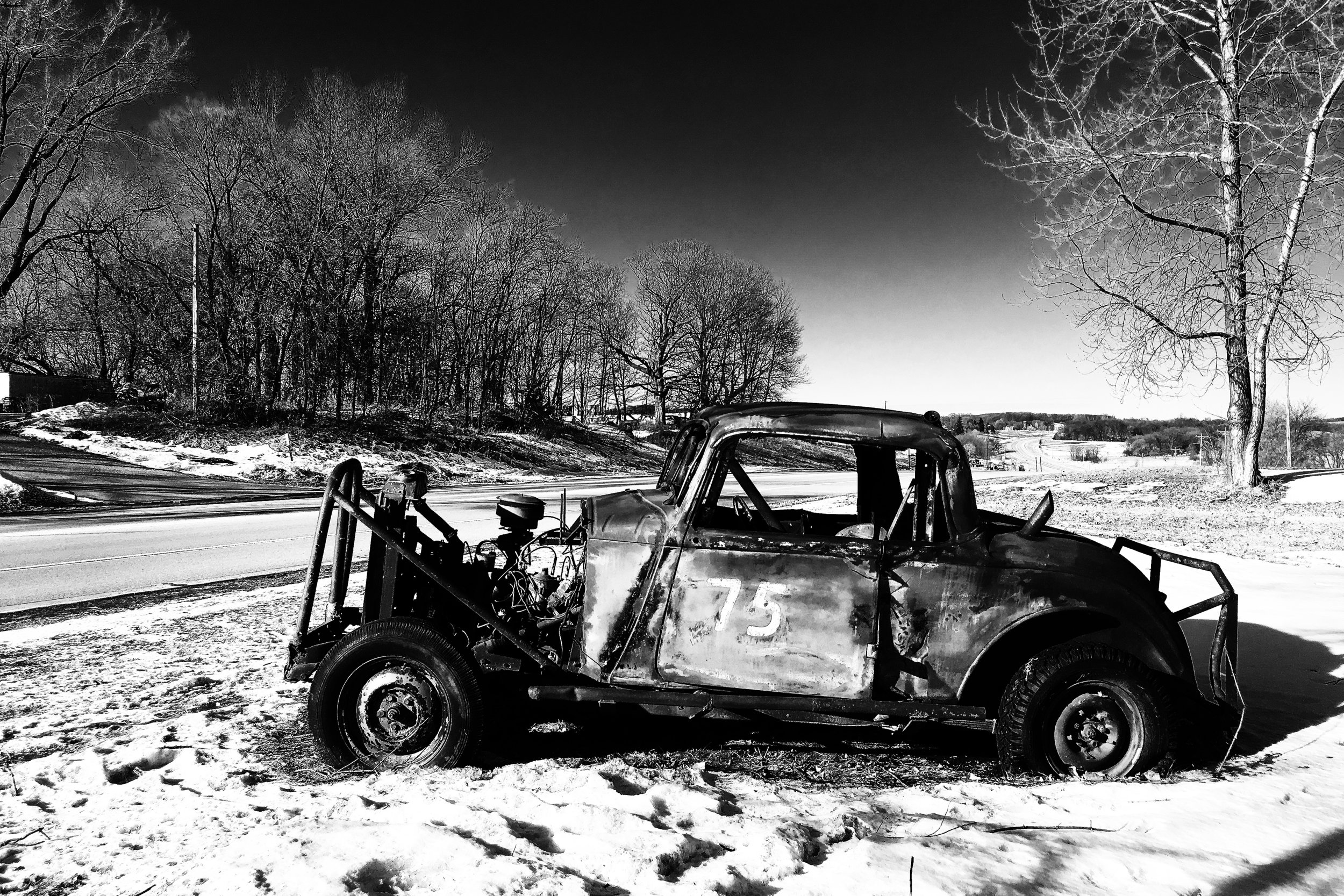
A little snow on a Tuesda
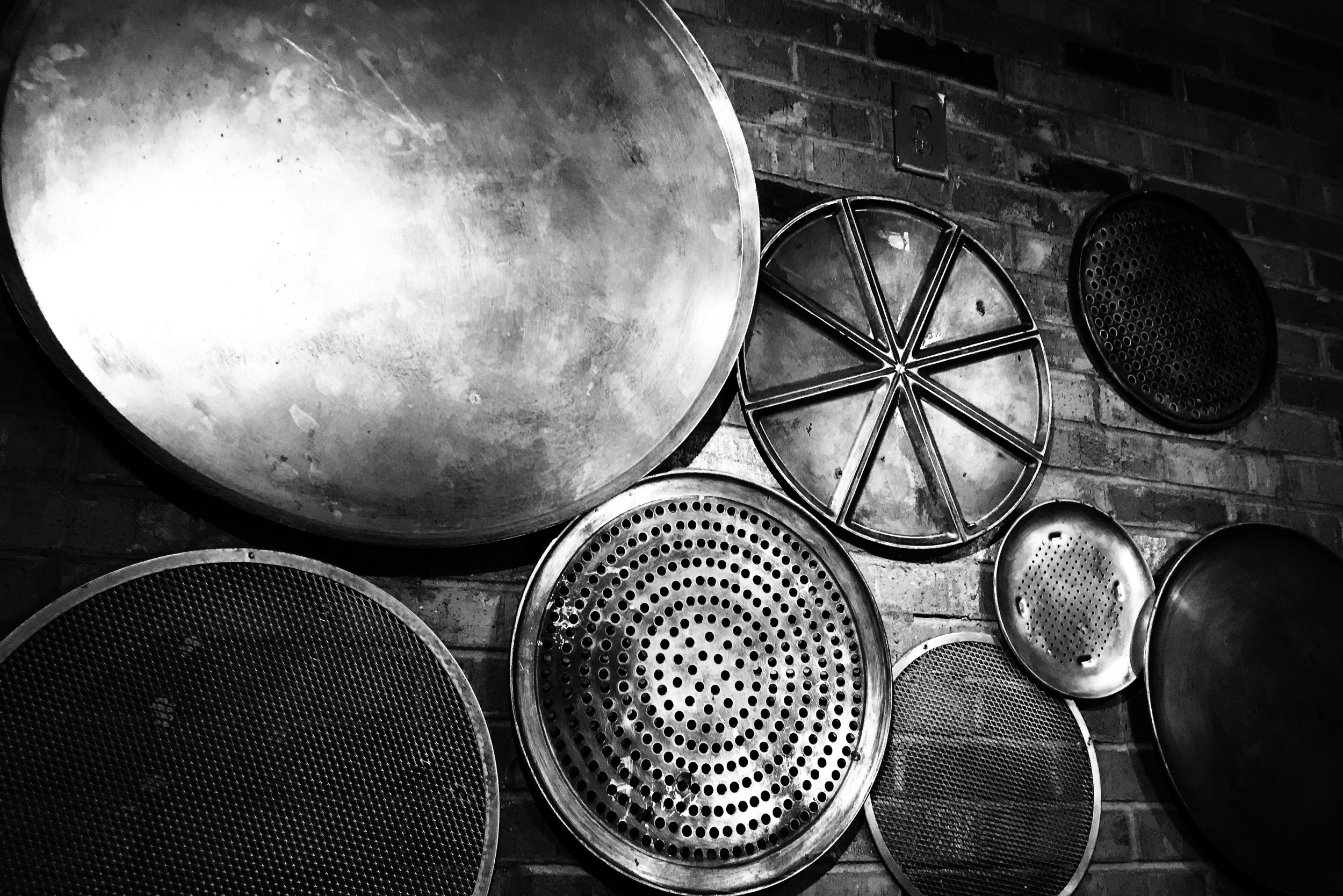
A quick trip to the metro


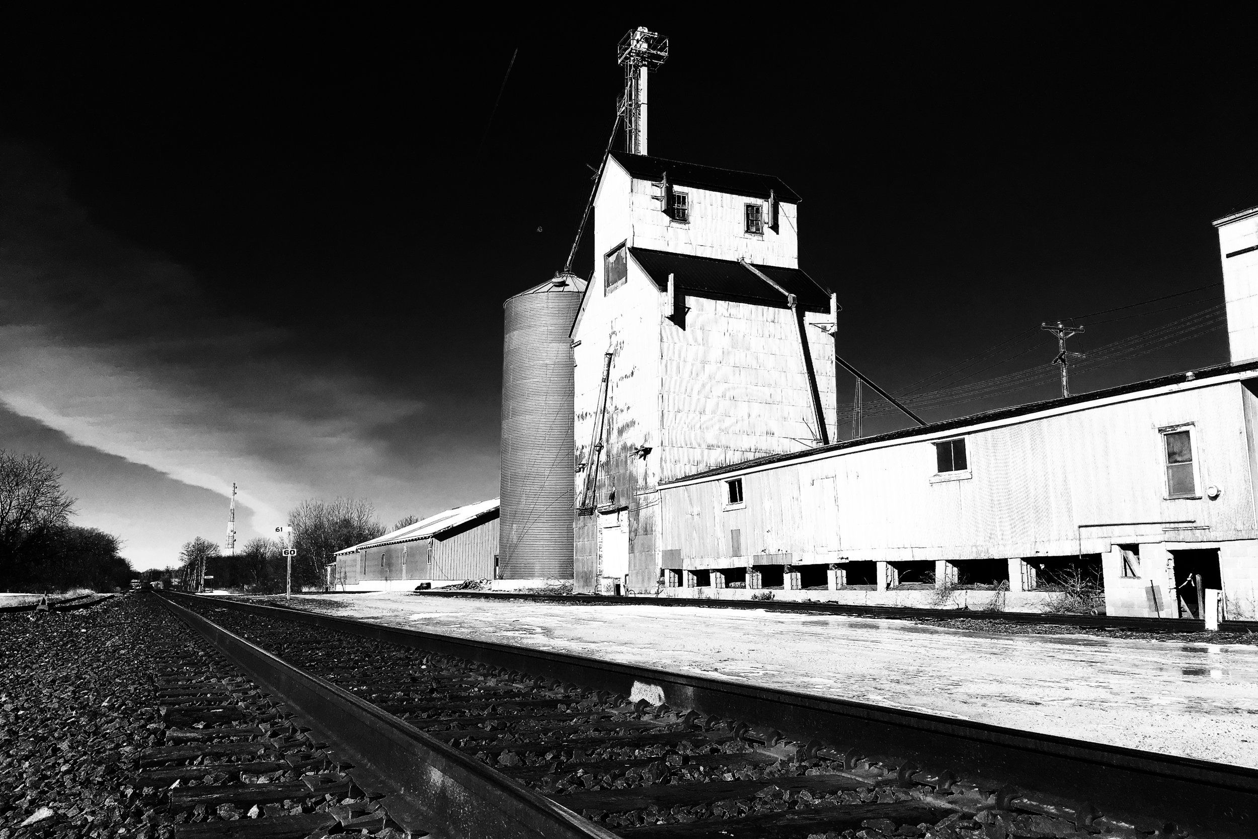
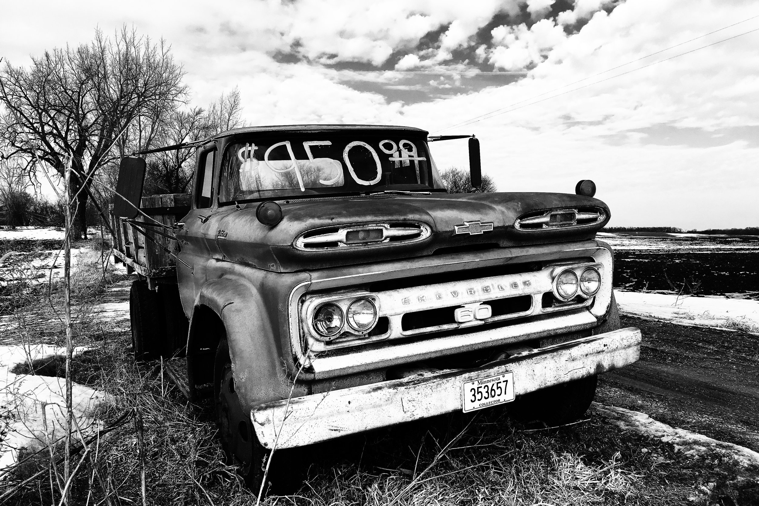
Another road trip


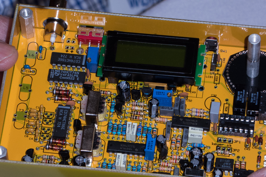
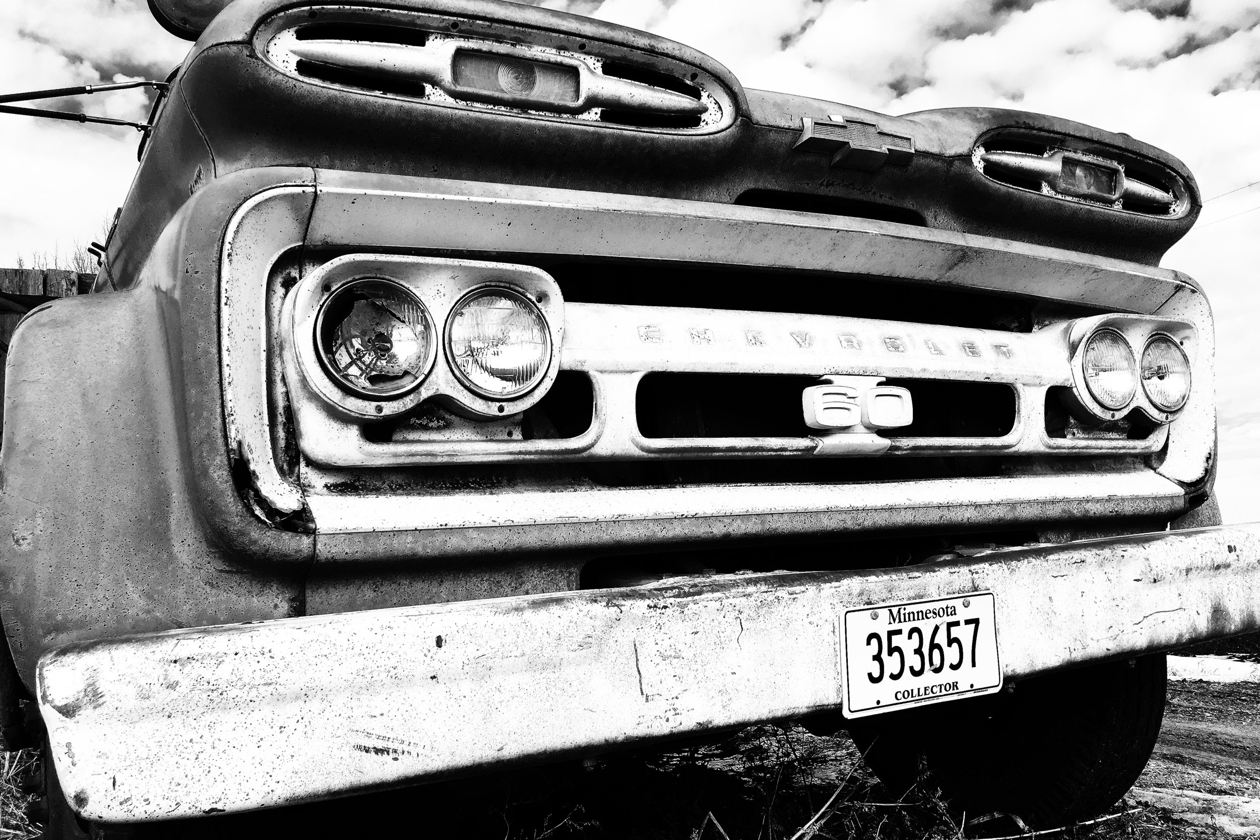
Trying something new

Mounting external speakers for mobile use can be a PIA. I noticed that a local ham had squeezed a speaker between the headrest and seat in his SUV. I liked that idea & it mostly worked until it didn’t and would occasionally pop loose. I decided that between my modest machine shop and 3D printer that I should be able to fab something.
I grabbed a caliper and measured the diameter of the headrest supports and the distance between the supports and head over to my CAD program (Fusion 360). It took about 10 minutes to draw up a model that I liked.
Here it is installed in my Jeep Patriot. Unless you were looking for it most people would never even know that it is there.
The install is crazy simple.
The print time was about 90 minutes and it cost about $1.75 in filament. It is attached using 4-40 screws and the plastic holes are tapped for threads. My total time investment was under two hours.
73 de NG0R
I always try to have a camera with me when I am out-and-about. Frequently I have a dSLR, almost always an iPhone 6s+, and more recently an 18mp Lumix point and shoot.
I had spent a rare day in the office in the metro so I had an extended evening drive back to our rural home. There were some scattered clouds which made a colorful sunset. I was on a conference call while driving so I put the call on mute, found a spot on a nearby gravel road to pull over and swing the Jeep into a position to take a few picture through the open window with the point-and-shoot camera.
The best best part was that it did not even disrupt the call or slow down the drive home. :-)
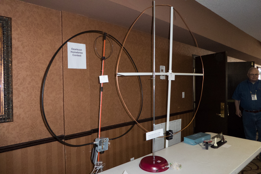
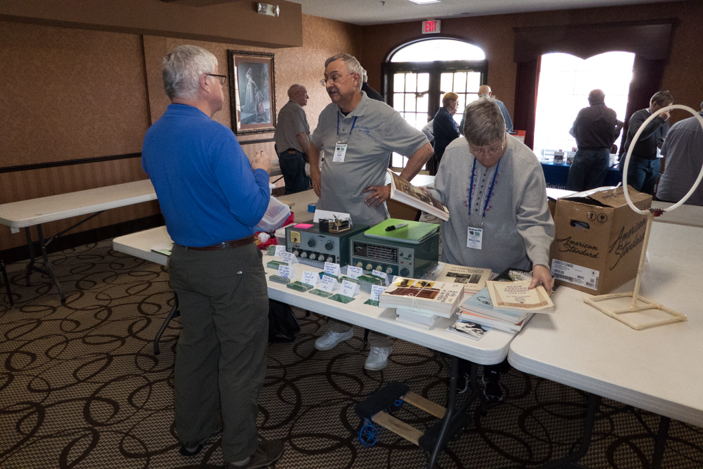
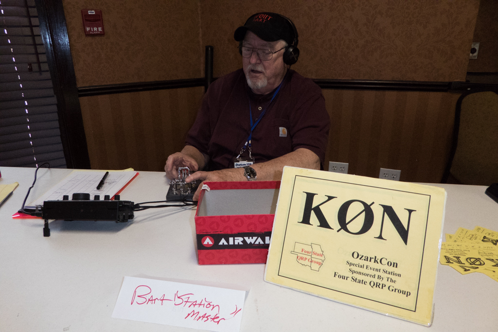
Another year, another road trip to Branson, more ham radio fun